Recently, in every industrial application a boost converter is mostly widely used, due to environmental reaction of utilizing nonrenewable energy and reducing of individual store have complete it mandatory to utilize clean and inexhaustible power sources [
1,
2]. The application of converter is in energies, PV (photovoltaic), wind and FC (fuelcell) are used as DG systems [
3]. These systems be naturally depending on atmosphere. For instance, in some systems, for increasing the output voltage PV cells are united in sequence, the dark effect cannot be obtained in this condition [
4]. For boost the output boost converter are used in this system, each PV panels can have controlled itself individually by connecting these converters, with smaller in size along with high conversion gain ratio and greater efficiency are the features of boost converters [
5]. For photovoltaic functions, maintaining low current ripples across the input side is also necessary. However traditional boost converter attains required HC (high conversion) ratio with greater D (duty cycle). Moreover, due to less transformation efficiency, reversal-recovery and Electro-magnetic- induction (EMI) troubles, the excess voltage gain will not have achieved [
6].
Now a day’s, many converter arrangements with various novel techniques has been discussed recently by achieving greater voltage gain and efficiency. There are few techniques which are switched capacitors and voltage lift for getting excess VG [
7]. Higher current ripples across the major switch are the significant fault of these converters which reducing the performance effectiveness and voltage increase of the converter [
8]. By getting high voltage increase the turns across the coupled inductor is adjusted. However, voltage spikes obtained across main switch because of leakage inductance, and it cause high power dissipation. The storage energy across the leakage inductor should be regained for eliminating such a problem. So, a voltage clamp is needed for such a type of designed converters. Various voltage clamps have been introduced for different coupled inductor-based converters. The major drawback is high input current ripples across the inductor [
9]. Due to small effective action of fuel cells, such type of converters is not applicable for these systems. High step up non isolated closed loop coupled inductor base converter has been introduced. By using a greater number of components is the main concern of all these converters, hence this paper discussed about SEPIC based converter has been introduced. The input side current rippled have be reduced due to owning the SEPIC converter has an inductor which is connected at source side [
10,
11].
A high step-up CI-based DC-DC power converter shown in . As shown in this picture, for reducing input current ripples inductor connected across the input side. Due to C1 and D1 the switching voltage is reduced. This gives a switch S with low on state-resistance Rdson to reduce the conduction losses [
12]. However, switching losses are reduced due to ZCS condition. The operation principle explained on given below.
The major contribution of this paper is as followed
1. Proposed a novel DC-DC converter for high gain applications along with mathematical modelling and design parameters.
2. A novel state space modelling technique is presented and analyzed for battery storage applications and EV applications.
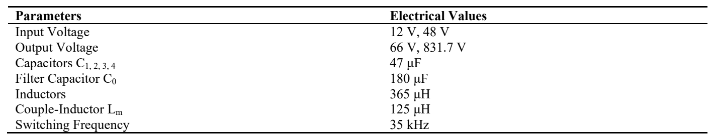
3. Detailed simulation model is presented for two different case conditions, case-1 is for 12 V to 66 V conversion with a D = 0.5, where in case-2 48 V to 831.7 V conversion with a D = 0.7.
. Non-Isolated HG DC-DC converter.
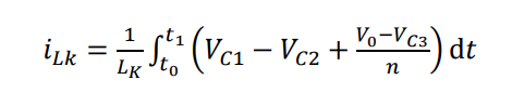
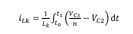
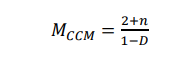
The operating principle and analysis of the closed loop DC-DC converter, during this entire derivation there are some ideal conditions to be consider. All capacitors and inductors are having the minimal voltage ripples and current ripples which are coming under 2% [
13]. The continuous and discontinuous conduction mode waveforms are presented in .
. Ideal waveforms for Proposed DC-DC converter: (a) CCM; (b) DCM.
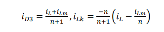
The main non-isolated DC-DC converter operation analyzed under CCM at single switching period consisting of five different time intervals. The current direction in the main converter and waveforms is shown in . The inductor current of the non-isolated CI is defined in Equation 1:
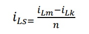
The inductor current and secondary sided non-isolated coupled inductor current cannot change synchronously. The complete operation and steady-state study of the non-isolated converter is discuss on below.
2.1.1. Mode I [
t0 <
t <
t1]
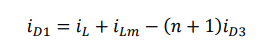
The main switch S and Diode D
3 is turned on.
iLk is increased to equal
iLm in this time interval. This mode ends when the
iLk &
iLm of the non-isolated coupled inductor are the same.
The equation of
iLk can be written as:
First mode of interval is very small and the
VLK is high, and the value of
LK is less. By the
V1 the inductor L is magnetized. After completed this time interval, the
NS current of the non-isolated coupled inductor as well as a result, the diode
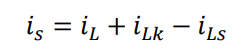
iD3 becomes to zero. Using KCL, the
iS can be written as:
. Interval [t0-t1] in Mode-1.
2.1.2. Mode II [
t1 <
t <
t2]
The switch is quiet on in this time interval and the circuit mode is shown in . The
iLm decreases linearly and exceed
iLk. The
iLk equation can be taken as follows:
The diode D
2 turns on due to flow of
NS current. Thus, Diode D
2 current increase gradually from zero. The C
3 is Energized Due to the
NS current of the non-isolated coupled inductor The stored power in capacitor C
1 is de-energized to the capacitor C
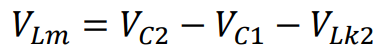
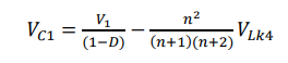
2 and coupled inductor. Due to the input power supply the inductor L is magnetized. This time interval completed when switch is in open circuited. In this time interval, by using KVL, the voltage equation can be obtained as follows
where
n =
NS/
NP. Interval [t1-t2] in Mode-2.
2.1.3. Mode III [
t2 <
t <
t3]
The inductor current
iL discharge through diode D
1 and it turns on similarly the switch is open circuited at this time interval and shown in . The D
1 and D
2 currents are written as:
The
iLk is de-magnetized continuously and its equals the
iLm. The
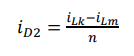
iD2 remains zero at this time interval.
iLK can be written as follows:
From above equation, a low value of leakage inductor and a high negative voltage creates its current slope to be high and it also present at small time interval. Due to the input source energy and de-magnetizing inductor L the capacitor C
1 is charged [
13,
14,
15,
16]. When diode D
2 is tuned off then this mode will be ends.
. Interval [t2-t3] in Mode-3.
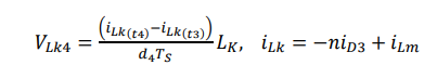
2.1.4. Mode IV [
t3 <
t <
t4]
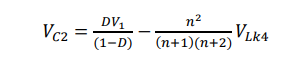
Due to V
1 and Inductor storage energy the capacitor C
1 is charged in this time interval and shown in . In this mode, the leakage inductor voltage will be altered. Its voltage equation will be able to taken as follows:
d4TS are time interval of this mode. Due to the
NS current of the non-isolated coupled inductor the C
0 is charged. The diode current D
1 will be written as:
when
iD1 becomes zero then this mode will be ends. However, the slope of
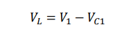
iLm is less than
iLK, according to equation (1), the slop
iD3 is +ve. In this mode the
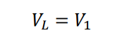
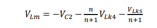
VL,
VLm, can be written as:
. Interval [t3-t4] in Mode 4.
2.1.5. Mode V [
t4 <
t <
t5]
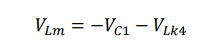
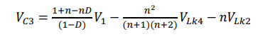
Diode D
3 is still on in this mode. Due to
iD3 the C
0 is energized. The
iD3 written as:
The diode D
3 and the
iLK slope calculate on the
iL,
iLM slope. Eliminating the
iL,
iLm ripples taking the slope of
iD3 and the
iLK becomes to zero. Then
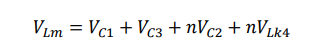
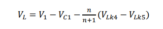
VLk will be zero. As stated in this equation, current is zero when S becomes on at the starting of mode one and shown in . So, under zero current the switch is short circuited. Using KVL the voltage equations be able to be taken as follows:
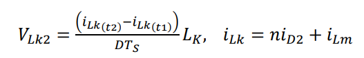
The slope of
iLk in modes 2 & 4 can be used to calculate
VLK2 &
VLK4. The non-isolated coupled inductor primary and secondary sides are in series with the capacitors C
2 and C
3,
iLk and
iLm avg. currents are zero, according to Amp-Sec balance principle. By applying balancing formulas on the C
1, C
2 &C
3, C
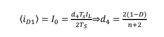
0 it can be justified that the io equal to the average value of diode current. Therefore, the following equation can be obtained from ,
So the
iripples of the
L and L
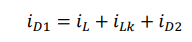
m are also in-considered in voltage gain computation. The
istress of the S and D
1 can be obtained as given below:
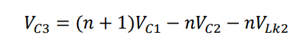
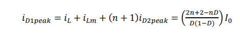
By in-considering the 3rd mode using this equation, the 4th time period can be obtained as
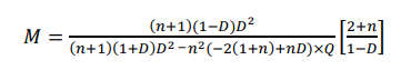
Due to (4) and (19) equations The voltage
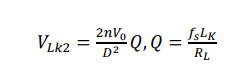
VLk2 can be found as:
where,
fswitch and
RL, respectively. Join Volt-Sec balance basis on the
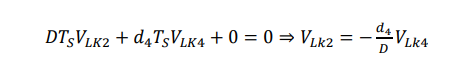
LK. By neglecting mode 1 and 3, the following equation is obtained.
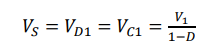
Applying Volt-Sec balance basis on the inductors the output is:
The
Vgain of proposed converter is
. Interval [t5-t6] in Mode-5.
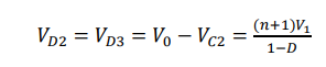
The voltage stresses of the switches/diodes can be formulated According to the operation principle of the new converter. To find the relevant semiconductors of the non-isolated DC-DC converter, the
VStress &
iStress should be obtained.
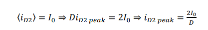
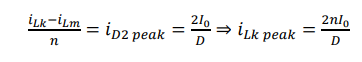
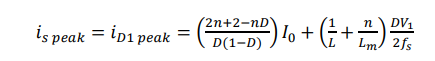
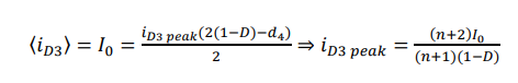
From equation (19) the D
2(peak) is obtained. The value of
Speak and diode D
1(peak) currents is as follows:
Based on and taking equation (32), the current value of D
3(peak) can be explained as given below:
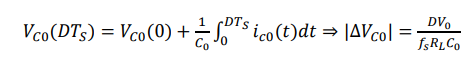
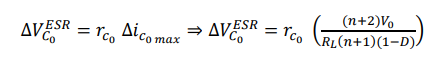
By neglecting the ESR of the C
0, the V
0 ripple of the new converter can be given as follow:
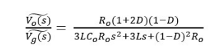
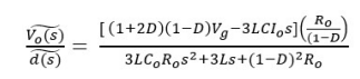
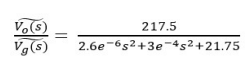
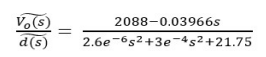
This section deals with the proposed state-space modelling technique to analyses the converter dynamic conditions [
14]. The control technique is derived from the input to output with respective to control the output of the converter and the transfer functions are derived as mentioned in the below. The inductors and capacitors are connected in parallel, hence all the components are named and derived as L, C using second order transfer function [
15].
Equations (36) and (37) denote the input to output relation and control to output transfer function, the frequency plots are drawn using the same equations and by using the original values the derived equations are in (38) and (39) respectively [
16]. denotes the frequency response plots of the system with proposed system.
. Bode Plot Stability Analysis.
This section gives a brief on simulation results and the performance analysis of proposed DC-DC converter for battery storage system application is presented in two different conditions. In the first condition converter is designed at a duty cycle of 0.5 with an input and output voltage parameters are showed in . In the second condition converter is designed at a duty cycle of 0.7 at different voltage conditions and parameters are showed in .
Table 1. Proposed Circuit Parameters.
shows the condition 1, where the converter is operating at in input voltage of 12 V at an output voltage of 48 V at a duty cycle of 0.5, and the other associated waveforms of switch voltage, diode voltage and capacitor voltage are presented. In the current waveforms of associated components like output current, inductor currents and diode currents are presented. From it illustrates the converter condition 2, which explains the converter adaptability at high voltage conversion from 48 V to 831.7 V along with switching voltage.
. Voltage Profile of Proposed DC-DC Converter.
. Current Profile of Proposed DC-DC Converter.
. At Different Voltage of Input and Output with D = 0.7.
A novel closed loop high step-up DC-DC converter with state-space controller for boost applications with stiff voltage regulation is presented in this paper. The new converter had major advantages like high voltage gain, low current ripples at input side and zero current switching, low Vstress at switch. The converter simulations are presented at two different conditions of duty cycles which is at D = 0.5 and 0.7. At all these conditions the converter is performed well and can be used as battery charger as well as auxiliary DC-DC converter for vehicle applications as well as PV systems.
This work is done in Vignan’s Foundation for Science and Technology and does not represent the views or opinions of author (Rajanand Patnaik Narasipuram) employer, Eaton. Eaton is the current address only and Eaton did not contribute to this work.
Not applicable.
Not applicable.
This research received no external funding.
The authors declare that they have no known competing financial interests or personal relationships that could have appeared to influence the work reported in this paper.