1. Introduction
As global industries push for sustainable and energy-efficient technologies, Wide-Bandgap (WBG) semiconductors such as silicon carbide (SiC) and gallium nitride (GaN) are increasingly recognized for their potential to revolutionize high-power and high-frequency applications. Their superior properties, including higher thermal conductivity, breakdown voltage, and energy efficiency, make them indispensable in electric vehicles (EVs), renewable energy systems, and 5G infrastructure [
1]. However, despite their advantages, the resource-intensive production processes of WBG semiconductors pose significant environmental challenges [
2]. The demand for these materials has surged in recent years due to their integration into critical energy applications. Still, concerns over the sustainability of their production and life-cycle remain unresolved. The rapid expansion of the semiconductor industry necessitates urgent consideration of how manufacturing practices can be improved to reduce carbon footprints, optimize energy consumption, and promote resource efficiency. This review examines sustainable manufacturing approaches, material recycling, and circular economy strategies to mitigate these environmental concerns, differentiating itself from previous studies that primarily focus on WBG material properties.
WBG semiconductors offer key advantages over traditional silicon-based devices. SiC has a wide bandgap of 3.26 eV, high thermal conductivity (4.9 W/cm·K), and a critical electric field strength ten times higher than silicon, making it ideal for high-temperature and high-voltage applications [
3]. Similarly, GaN has a bandgap of 3.4 eV, high electron mobility, and superior power density, making it suitable for high-frequency electronics [
4]. These properties enable WBG semiconductors to enhance power conversion system efficiency significantly, reducing energy losses and promoting sustainability in photovoltaic inverters, wind turbines, and EV powertrains [
5]. Beyond SiC and GaN, emerging WBG materials such as gallium oxide (Ga
2O
3) and diamond exhibit unique properties for specialized applications. Ga
2O
3, with a bandgap of around 4.8 eV, enables extreme high-voltage applications, while diamond, with a 5.5 eV bandgap, offers exceptional thermal conductivity [
6]. These next-generation materials are expected to complement SiC and GaN in high-power electronics, offering solutions that balance performance, longevity, and sustainability.
Despite their technological benefits, the production of WBG semiconductors is energy-intensive and environmentally taxing. Epitaxial growth techniques such as chemical vapor deposition (CVD) and molecular beam epitaxy (MBE) demand high temperatures, leading to substantial greenhouse gas emissions [
7]. The extraction of raw materials such as gallium contributes to ecological degradation and supply chain vulnerabilities, as China controls a major portion of WBG material production [
8]. The energy-intensive purification processes required to produce high-quality WBG materials further exacerbate their environmental impact. The industrial-scale manufacturing of WBG devices results in significant waste generation, including toxic by-products, requiring advanced mitigation strategies. Companies are increasingly exploring green synthesis methods, including lower-temperature deposition techniques and alternative solvents, to minimize chemical waste and energy consumption while maintaining high material purity levels.
End-of-life disposal presents another sustainability concern. Current recycling methods for SiC and GaN remain inefficient, leading to substantial electronic waste (e-waste). The improper disposal of WBG materials can cause hazardous substances to leach into the environment, posing health risks [
9]. Addressing these issues requires innovative recycling strategies and regulatory frameworks. Implementing closed-loop recycling systems for reclaiming valuable semiconductor materials has been proposed as a viable solution, yet widespread adoption remains limited due to economic and technological barriers. The global semiconductor industry must enhance collaboration between manufacturers, policymakers, and research institutions to develop efficient e-waste processing methods and improve material recovery from discarded electronic devices.
While previous studies have primarily focused on the performance advantages of WBG semiconductors, fewer have examined their sustainability challenges and mitigation strategies. This review aims to assess the environmental impact of WBG semiconductor manufacturing through life-cycle analysis, explore energy-efficient fabrication methods, including low-energy epitaxial growth techniques, examine circular economy practices, such as WBG material recycling and waste reduction [
10], and identify future research directions for improving the sustainability of WBG semiconductor production. A key contribution of this review is its integration of recent advancements in sustainable semiconductor manufacturing, providing a holistic perspective that combines material science, industrial engineering, and environmental policy. The paper also highlights ongoing initiatives by semiconductor companies to adopt greener supply chain practices, aiming to reduce reliance on nonrenewable raw materials and optimize logistics to decrease overall carbon emissions.
Understanding the trade-offs between performance optimization and sustainability is crucial for guiding future innovations in semiconductor technology. Given the increasing reliance on WBG materials in emerging energy applications, finding ways to enhance their recyclability, reduce environmental footprints, and streamline supply chains will be essential. The review will analyze existing challenges and propose strategic recommendations for industry-wide sustainability improvements.
This paper discusses recent advancements in WBG semiconductor technologies, focusing on their applications in high-power and energy-efficient industries. It analyzes current sustainability initiatives, including green manufacturing techniques and circular economy strategies, and explores challenges associated with WBG semiconductor production, from raw material extraction to life-cycle management. The paper also outlines future prospects for sustainable semiconductor development and strategic steps to align with global sustainability goals. By presenting a holistic analysis of sustainable WBG semiconductor manufacturing, this review serves as a critical reference for researchers, industry stakeholders, and policymakers seeking to promote sustainable semiconductor manufacturing and reduce the ecological footprint of next-generation electronics.
2. Semiconductor Fundamentals and Historical Development
2.1. Introduction to Semiconductors
Semiconductors are essential materials characterized by their electrical conductivity, which lies between that of conductors and insulators, making them vital for controlling electric current in electronic devices [
11]. They are classified into intrinsic semiconductors, which are pure, and extrinsic semiconductors, which are doped with impurities to enhance conductivity [
12]. Among the semiconductors, silicon is used extensively due to its high-temperature stability and effective doping capabilities, allowing for the creation of both p-type and n-type semiconductors [
12,
13]. However, the increasing demand for more energy-efficient and sustainable electronic systems has exposed silicon’s limitations in high-power and high-temperature applications, driving the transition toward Wide-Bandgap (WBG) semiconductors [
13,
14]. While silicon-based semiconductors have shaped modern electronics, their high energy consumption, material waste, and limited efficiency in power applications have raised sustainability concerns. WBG semiconductors offer superior performance in high-power applications, significantly reducing energy losses and carbon footprints. Their ability to operate at higher voltages and temperatures without excessive cooling requirements makes them a crucial advancement for sustainable energy applications, including electric vehicles (EVs), renewable energy systems, and power grids [
7,
15].
2.2. The Shift to Wide-Bandgap (WBG) Semiconductors
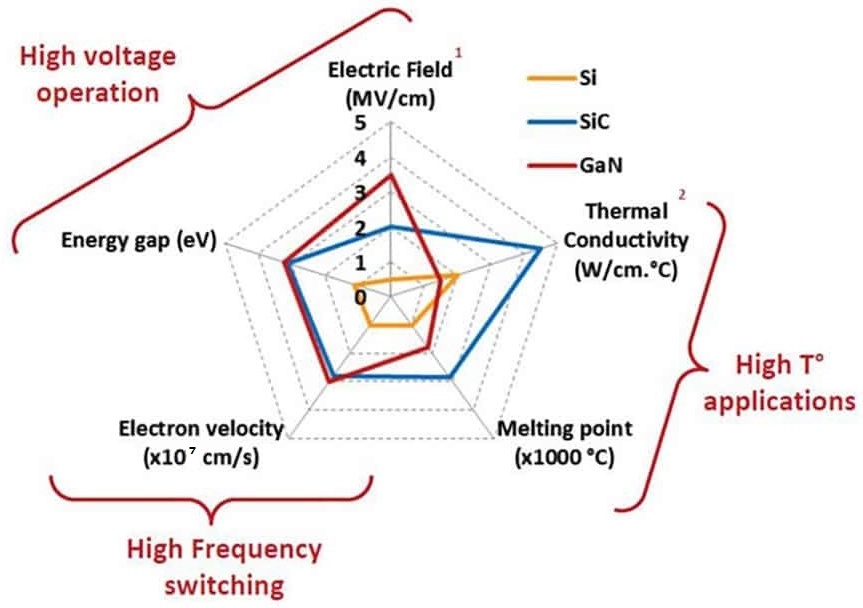
The increasing demand for more efficient, reliable, and high-performance electronic systems has driven a transition from traditional silicon-based semiconductors to Wide-Bandgap (WBG) technologies. Wide-bandgap (WBG) semiconductors like Silicon Carbide (SiC) and Gallium Nitride (GaN) outperform Silicon (Si) by offering significantly larger bandgaps—around 3.26 eV for SiC and 3.4 eV for GaN (, ), allowing them to function at much higher voltages, temperatures, and frequencies while reducing energy losses and minimizing thermal degradation [
16]. These properties have made WBG semiconductors the preferred choice in high-power applications [
17].
. Materials Properties of WBG semiconductors (SiC, GaN) compared to Si presented in a spider chart. The chart maps key properties, including electric field (MV/cm), thermal conductivity (W/cm·°C), melting point (×1000 °C), electron velocity (×10⁷ cm/s), and energy gap (eV). The numbers 1–5 represent the scale or intensity of each property. Superscripts: <sup>1</sup> Indicates materials properties relevant to high-voltage operation, and <sup>2</sup> Indicates properties important for high-temperature applications.
Beyond their electrical performance, WBG materials are more sustainable than traditional silicon-based devices. The adoption of SiC in electric vehicle powertrains has significantly improved efficiency, as seen in Tesla’s Model 3, which utilizes SiC-based inverters to extend driving range while minimizing thermal losses [
18,
19]. Similarly, GaN has been widely adopted in high-frequency power conversion applications, enabling more compact and energy-efficient solar inverters and power grids [
6]. This transition is pivotal in achieving a more sustainable electronics industry by reducing material waste, energy consumption, and overall carbon emissions [
5,
6].
2.3. Fundamental Properties of Wide-Bandgap (WBG) Semiconductors
WBG semiconductors possess unique material properties, making them superior to traditional silicon devices in power applications. With their inherent characteristics, WBG devices can function effectively at temperatures up to 300 °C, far exceeding the 150 °C limit of traditional silicon devices [
16,
18]. Their superior material properties, including high thermal conductivity, high critical electric fields, and reduced conduction losses, make them ideal for various applications [
6,
20].
Silicon carbide (SiC) exhibits a thermal conductivity of approximately 4.9 W/cm·K, which is significantly higher than silicon’s 1.5 W/cm·K (, ), making SiC particularly advantageous for high-temperature applications such as electric vehicle powertrains due to its effective heat dissipation capabilities [
16,
21]. In contrast, gallium nitride (GaN) has a lower thermal conductivity of about 1.3 W/cm·K, but its higher electron mobility (up to 2000 cm
2/V·s) () allows for enhanced efficiency in high-frequency switching applications, such as 5G networks and radar systems [
22,
23]. However, the thermal management of GaN-based devices remains critical, as self-heating effects can lead to performance degradation [
24].
A life-Cycle Assessment (LCA) of semiconductor materials indicates that WBG semiconductor devices, such as silicon carbide (SiC) and gallium nitride (GaN), significantly enhance the efficiency of power electronics, achieving over 30% reduction in power losses compared to traditional silicon-based devices [
5]. These materials enable higher switching speeds, greater power densities, and improved thermal performance, allowing for smaller and lighter power converters, which in turn reduce raw material consumption and enhance recyclability [
25]. Ongoing research is focused on developing environmentally friendly recycling processes for WBG semiconductors and promoting a circular economy in electronic manufacturing. The integration of a parametric life-cycle assessment (PLCA) model in the design phase can further optimize the environmental impacts of these technologies, ensuring sustainable practices in the power electronics sector [
26].
The integration of SiC and GaN into power electronics has revolutionized modern energy infrastructure, contributing to the sustainability of electric grids, solar inverters, and energy storage systems. These advancements highlight WBG semiconductors’ essential role in reducing energy consumption, minimizing waste, and ensuring more efficient power conversion in future electronic systems [
7].
.
Physical properties of Silicon (Si), Silicon Carbide (SiC) and Gallium Nitride (GaN) [27].
| Electrical Property |
Si |
4H-SiC |
GaN |
| Bandgap energy (eV) |
1.1 |
3.26 |
3.4 |
| Thermal Conduction (W/cm·K) |
1.5 |
4.9 |
1.3 |
| Electron Mobility (cm2/V·s) |
1300 |
900 |
900–2000 |
| Saturation drift velocity |
1 × 10⁷ |
2 × 10⁷ |
2.5 × 10⁷ |
2.4. Historical Development of Wide-Bandgap (WBG) Semiconductors
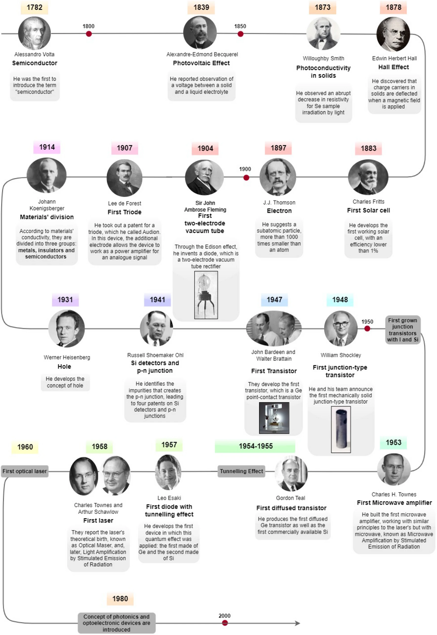
The history of semiconductors is encapsulated by major discoveries, starting with Alessandro Volta, who, in 1782, coined the term “semiconductor”, providing a name that would form the groundwork for other explorations to come () [
27]. The photovoltaic effect, discovered by Alexandre-Edmond Becquerel in 1839, was pivotal for modern solar technology, culminating in Charles Fritts’ creation of the first solar cell in 1883 using selenium () [
28]. In the early 20th century, Sir John Ambrose Fleming was credited for pioneering the invention of the vacuum tube in 1904 (). This was then followed by the discovery of the first commercial silicon transistor by John Bardeen and Walter Brattain in 1947 (), establishing silicon as the dominant semiconductor material [
13]. However, by the 1990s, silicon’s limitations in high-power and high-temperature applications prompted research into alternative materials like silicon carbide (SiC) and gallium nitride (GaN), which were recognized as Wide-Bandgap semiconductors [
12,
29]. This evolution reflects the ongoing quest for improved semiconductor performance and applications.
. Timeline of the most historical milestone throughout the last centuries [
28].
2.4.1. Emergence of SiC and GaN
Silicon Carbide (SiC) power devices, developed in the 1990s, have significantly transformed the semiconductor industry by enabling high-temperature applications due to their exceptional properties, such as high thermal conductivity and electric field strength, making them ideal for power electronics in electric vehicles and renewable energy systems [
15,
30]. Concurrently, Gallium Nitride appeared in the early 2000s as a key material for high-frequency electronics with better breakdown voltage and switching speed than traditional silicon semiconductors, making it crucial for high-performance applications [
16]. The advancements in Wide-Bandgap (WBG) materials like SiC and GaN enhance efficiency and allow operation at higher voltages and temperatures, facilitating innovations in power management systems and contributing to sustainability efforts within the technology sector [
31]. This evolution in semiconductor technology marks a pivotal shift, driving the development of more efficient and reliable power electronics.
2.4.2. Pivotal Technological Advancements
The Power Electronic Building Block (PEBB) program, initiated in 1994, significantly advanced Silicon Carbide (SiC) technology by focusing on reducing the size, weight, and cost of military power electronics, which also benefited commercial sectors like electric vehicles [
32]. SiC devices have shown remarkable capabilities, handling voltages up to 20 kV, making them ideal for applications in electric vehicle powertrains and energy storage systems [
16]. Concurrently, Gallium Nitride (GaN) devices have gained traction for their efficiency in power conversion, particularly in electric vehicles where compact and energy-efficient designs are essential [
16]. By the mid-2000s, Wide-Bandgap (WBG) semiconductors, including SiC and GaN, demonstrated significant performance enhancements, with GaN devices achieving switching frequencies up to 2 MHz, which is beneficial for fast chargers and RF amplifiers [
16,
33]. This synergy between military and commercial applications has propelled the development of advanced power electronics technologies.
2.4.3. Impact on Modern Applications
The integration of Wide-Bandgap (WBG) semiconductors has considerably modernized applications in contemporary electric vehicle and renewable energy sectors. Their superior properties enable more efficient and compact power management systems, thereby enhancing the vehicle’s performance and range in EVs [
16,
20]. In renewable energy systems, SiC devices have notably improved the efficiency of photovoltaic inverters, minimizing energy losses and costs associated with solar energy conversion [
18]. Furthermore, GaN and SiC are pivotal in revolutionizing power supply systems by reducing energy losses during conversion processes and contributing to sustainability efforts to lower carbon footprints [
34,
35]. Emerging WBG materials like aluminum phosphide, diamond, and boron nitride also show promise due to their superior properties, such as high thermal conductivity and breakdown strength, which are essential for high-power applications in extreme environments [
36]. Collectively, all these developments contribute to the global efforts aimed at tackling modern energy-related problems and minimizing the carbon footprint [
16,
20].
2.4.4. Evolution Toward Sustainable Manufacturing
The transition to sustainable manufacturing is crucial in WBG semiconductor manufacturing since the sector involves highly energy-intensive processes with environmentally toxic by-products. The integration of Industry 4.0 technologies, including Internet of Things (IoT), Artificial Intelligence (AI), and automation, plays a vital role in reducing energy consumption, optimizing resource use, and minimizing waste [
37,
38]. Advanced data-driven approaches like machine learning and real-time energy monitoring allow semiconductor fabs to analyze energy usage patterns and implement targeted interventions to optimize efficiency [
39,
40]. Furthermore, simulation and AI-driven decision-support tools enhance resource management, contributing to significant reductions in greenhouse gas emissions and promoting sustainable production [
41,
42].
In semiconductor manufacturing, AI-driven process optimization has enabled manufacturers to reduce energy waste and improve yield efficiency through real-time monitoring systems. The implementation of IoT-based predictive maintenance also plays a critical role in reducing material waste and enhancing overall sustainability [
38,
43]. The development of sustainable IoT systems, such as the SUPERIOT project, emphasizes eco-friendly materials and energy-harvesting technologies, aligning with broader sustainability goals [
44]. The integration of AI, IoT, and automation in WBG semiconductor manufacturing represents a major step toward a more sustainable and environmentally friendly industry [
8,
45].
2.4.5. Environmental Impact of Manufacturing
The semiconductor industry is a significant contributor to carbon emissions and water consumption, necessitating the adoption of innovative sustainability strategies. Carbon emissions in semiconductor fabs primarily arise from energy consumption and the use of fluorinated compounds, which are potent greenhouse gases [
45,
46]. Strategies to reduce these emissions include transitioning to renewable energy sources and improving energy efficiency in fabrication processes [
47]. However, despite these efforts, the industry’s overall emissions continue to grow, highlighting the need for more aggressive emission reduction commitments and cleaner manufacturing technologies.
Water usage is another major concern in semiconductor production, as fabs consume vast amounts of ultrapure water (UPW). Some facilities use over 2 million gallons per day for wafer processing, making water recycling and reclamation critical strategies for reducing demand on municipal water systems [
48,
49]. Technologies such as reverse osmosis and ceramic membrane filtration have improved water recycling rates, helping environmental impacts [
50,
51]. Furthermore, the reuse of de-ionized water can significantly reduce water consumption and associated carbon emissions, though it requires careful management to balance water savings with energy use [
52]. As the semiconductor industry expands globally, particularly in regions like China and Southeast Asia, these sustainability strategies will be crucial in mitigating environmental impacts [
53].
2.4.6. Current Innovations
Innovations in WBG semiconductor manufacturing are addressing environmental challenges through closed-loop recycling systems and green chemistry principles. Closed-loop recycling systems enable the recovery of valuable materials from end-of-life (EoL) WBG devices, reducing reliance on virgin raw materials and minimizing environmental impact [
54]. With GaN substrate recycling, a laser slicing process has been developed to recover GaN substrates, allowing their reuse in power device fabrication without degrading structural or electrical properties () [
54]. Researchers have successfully extracted indium, gallium, and germanium from spent LEDs, LCDs, and photovoltaics using hydrometallurgical and biohydrometallurgical methods, achieving recovery rates above 95% for indium and 99% for gallium () [
55,
56]. Recycling selenium-based optoelectronic devices are possible through a closed-space evaporation process that recovers 98% of selenium and 100% of gold electrodes from end-of-life photovoltaic devices () [
57].
.
Comparison of Recycling Methods for WBG Semiconductors [54,55,56,57].
| Material/Device |
Recycling Method |
Efficiency/Yield |
| GaN substrates |
Laser slicing |
No degradation |
| Indium (from LCDs) |
Mineral acid leaching |
Over 95% recovery |
| Gallium (from GaN LEDs) |
HCL leaching after annealing |
99% recovery |
Selenium
(from photovoltaics)
|
Closed-space evaporation |
98% for selenium,
100% for gold
|
2.4.7. Integration of Industry 4.0 and Reconfigurable Technologies
The integration of Industry 4.0 technologies, such as Smart Sensors, Cyber-Physical Systems (CPS), the Internet of Things (IoT), and Artificial Intelligence (AI), is revolutionizing manufacturing processes by enhancing resource management and minimizing emissions, particularly in semiconductor production [
58,
59]. These intelligent manufacturing systems facilitate real-time data analysis and automation, allowing adaptive manufacturing to swiftly respond to changing market demands [
60,
61]. Reconfigurable technologies play a crucial role in this transformation, enabling manufacturers to fine-tune their processes dynamically, boosting production efficiency and significantly reducing waste and environmental impact [
58,
62]. By leveraging these advanced technologies, industries can achieve higher operational effectiveness and sustainability, positioning themselves competitively in the evolving digital landscape [
59,
60]. Automation and robotics further enhance efficiency by minimizing human intervention in wafer handling, assembly, and packaging, thereby improving yield and reducing scrap materials [
63]. Reconfigurable IC designs and 3D-integrated circuits (3D-ICs) support modular electronics, enabling component reuse and reducing electronic waste [
64].
2.4.8. Toward a Circular Economy
The semiconductor industry embraces circular economy principles by prioritizing resource optimization and waste minimization across the product life-cycle. Blockchain, IoT, and AI are being utilized to enhance supply chain transparency and facilitate material reuse [
65]. Companies have implemented recycling programs and resource recovery initiatives, demonstrating industry-wide commitment to sustainability [
66,
67]. By integrating advanced recycling technologies, green chemistry principles, and Industry 4.0 solutions, the semiconductor industry is moving toward a more sustainable and circular economy, ensuring long-term viability and environmental responsibility [
68,
69].
3. WBG Semiconductor Manufacturing
3.1. GaN and SiC Semiconductor Manufacturing Route
3.1.1. GaN Manufacturing Route
The manufacturing of gallium nitride (GaN) involves several critical steps to ensure the formation of high-quality layers suitable for advanced electronic applications. The process begins with substrate preparation, where materials like sapphire, silicon, and silicon-on-insulator (SOI) are cleaned and patterned to create a defect-free surface for GaN growth [
70]. Epitaxial growth, primarily achieved through Metal-Organic Chemical Vapor Deposition (MOCVD), facilitates the deposition of GaN from metal-organic precursors at elevated temperatures, often utilizing a buffer layer to enhance the quality of the film [
35,
71]. To improve sustainability, low-temperature MOCVD techniques and Atomic Layer Deposition (ALD) are being implemented to minimize energy consumption and carbon emissions, thereby reducing the environmental footprint of GaN manufacturing [
72,
73].
Doping is performed via ion implantation techniques, where elements like magnesium are introduced to achieve p-type conductivity and nitrogen plasma treatments help enhance carrier activation [
74]. The adoption of alternative, less-toxic precursors in doping processes aligns with green chemistry principles, further minimizing the ecological impact of semiconductor manufacturing [
72]. Closed-loop water recycling systems have been introduced to reduce water and chemical usage in GaN growth processes, making them more environmentally sustainable [
48].
3.1.2. SiC Manufacturing Route
Silicon Carbide (SiC) substrates are primarily produced using the physical vapor transport (PVT) technique, which ensures high-quality single-crystal formation and addresses the limitations of melt-based growth methods [
75,
76]. Following substrate production, wafers undergo chemical-mechanical polishing (CMP) to ensure surface smoothness before subsequent epitaxial growth via Chemical Vapor Deposition (CVD) [
75,
77]. Recent advancements in low-temperature CVD techniques are being adopted to reduce energy consumption, significantly improving sustainability in SiC fabrication [
78].
Doping in SiC is typically achieved through ion implantation (nitrogen for n-type, aluminum for p-type), necessitating precise control to maintain material integrity while optimizing device efficiency [
79]. Advances in alternative doping strategies, such as plasma-assisted doping and solid-phase diffusion, are emerging as energy-efficient, lower-waste solutions [
80]. Innovations in micro-powder recycling through alkali wash and pickling have provided a sustainable method to recover SiC material while maintaining high device performance [
81].
To further enhance sustainability, water purification and reuse technologies have been integrated into SiC fabs, reducing ultrapure water and sulfuric acid consumption [
48]. Moreover, the adoption of renewable energy sources and carbon capture technologies in SiC production is helping to achieve negative emissions, significantly lowering the carbon footprint of SiC manufacturing [
82].
3.2. Innovations in WBG Semiconductor Manufacturing
The growing demand for Wide-Bandgap (WBG) semiconductors, including silicon carbide (SiC), gallium nitride (GaN), and ultrawide-bandgap (UWBG) materials like gallium oxide (Ga
2O
3), has necessitated a shift toward sustainable manufacturing practices. With concerns over raw material scarcity and energy consumption, comprehensive life cycle assessments (LCA) are being conducted to identify environmental hotspots in WBG production [
83]. Key innovations in sustainable WBG semiconductor manufacturing include green chemistry, AI-driven process optimization, and advanced recycling techniques [
84,
85,
86].
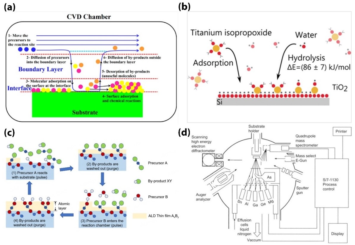
Several low-energy deposition techniques are being explored to reduce the energy burden of semiconductor manufacturing. Low-temperature Chemical Vapor Deposition (CVD) (b) minimizes energy use while maintaining high-quality material growth, unlike traditional Chemical Vapor Deposition (a), which is energy-intensive [
87,
88,
89]. Atomic Layer Deposition (ALD) (c) enables precise control over film thickness, reducing material waste and power consumption [
72]. Molecular Beam Epitaxy (MBE) (d) enhances material purity while operating at lower temperatures, significantly cutting down on energy requirements [
90]. Green chemistry approaches are being implemented to replace hazardous chemicals like hydrogen fluoride (HF) in WBG processing. The use of aliphatic amino acids as corrosion inhibitors in CMP slurries is one such advancement, reducing reliance on environmentally harmful chemicals [
78,
91].
. (<b>a</b>) Schematic of the main steps of the CVD process [
92]; (<b>b</b>) Schematic Diagram of ALD type reaction to a high Vacuum Low-temperature CVD process [
93]; (<b>c</b>) The reaction process of ALD [
94]; (<b>d</b>) Typical MBE system [
95].
As WBG semiconductor demand increases, sustainable material recovery and recycling methods are becoming critical. Recycling initiatives include the recovery of gallium and silicon from production by-products through advanced chemical separation techniques [
96]. For instance, the recycling of GaN, a refractory e-waste material, involves chemical pretreatment and thermodynamic processes to recover gallium, aligning with urban mining initiatives and international recycling directives [
97]. Closed-loop recycling systems reintegrate reclaimed materials back into the manufacturing cycle, reducing reliance on virgin raw materials [
98].
The integration of Industry 4.0 technologies, such as artificial intelligence (AI), machine learning, and digital twin simulations, is significantly enhancing the sustainability of wide bandgap (WBG) manufacturing. AI-driven process optimization has been shown to reduce energy consumption by 30% and improve material efficiency. AI technologies enable dynamic adaptation to changing conditions, reduce variability, and enhance quality through predictive maintenance and real-time monitoring [
95,
96]. The Internet of Things (IoT) plays a crucial role in predictive maintenance by monitoring equipment performance and predicting breakdowns, which minimizes downtime and reduces waste from defective products [
37,
96]. Digital twin simulations further contribute to sustainability by allowing semiconductor fabs to model production processes, thereby optimizing operational efficiency and energy use [
99]. These digital twins, supported by IoT and AI, provide real-time insights and enable continuous improvement in production processes, reducing downtime and enhancing maintenance strategies [
99]. The integration of AI and IoT in manufacturing not only enhances operational efficiency but also supports sustainable practices by lowering expenses, increasing productivity, and decreasing waste [
37].
With the rising demand for WBG semiconductors, concerns over ethical material sourcing have emerged. The industry is increasingly adopting traceability systems to ensure sustainable procurement of materials like gallium and silicon, addressing environmental degradation and human rights concerns [
100]. Government regulations such as the European Green Deal and U.S. federal incentives encourage investments in energy-efficient semiconductor technologies [
101].
4. Applications of Wide-Bandgap (WBG) Semiconductors in Sustainable Technologies
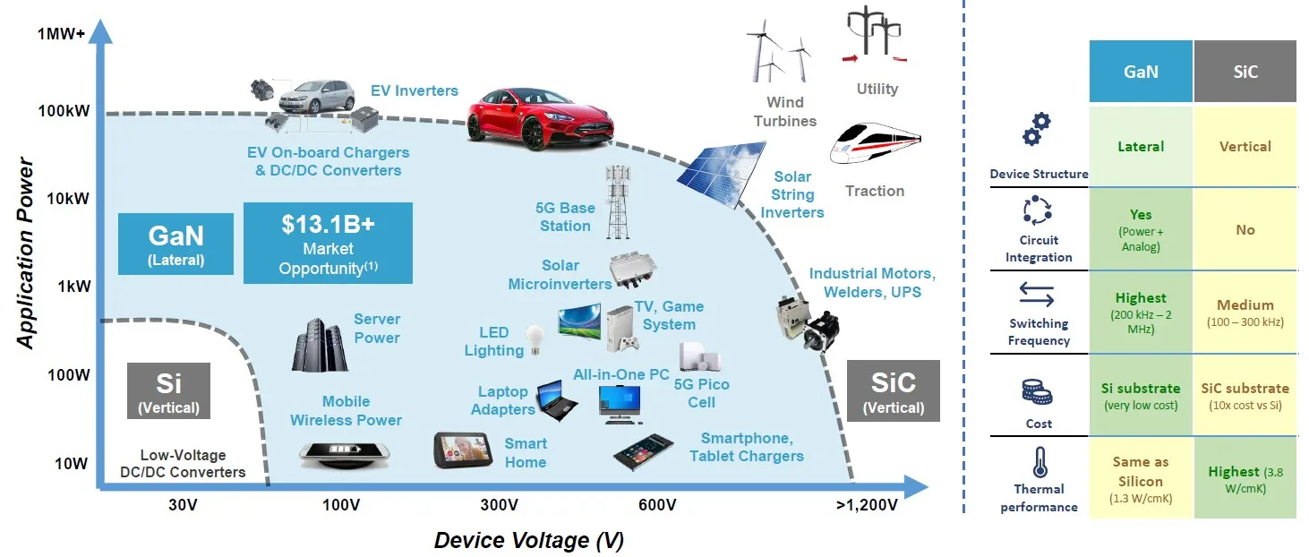
Wide-bandgap (WBG) semiconductors have gained significant attention for their transformative impact on various industries, especially in the pursuit of sustainable technologies. These materials are driving innovation in electric vehicles (EVs), renewable energy systems, 5G infrastructure, smart grids, and other crucial applications (). The integration of SiC and GaN in these technologies contributes to improved energy efficiency, reduced carbon emissions, and overall sustainability.
. Si, SiC, and GaN opportunities (Source: Power Electronics News) [
102].
Silicon Carbide (SiC) devices are transforming electric vehicle (EV) power systems () by significantly enhancing the efficiency of inverters and power modules. These components outperform traditional silicon systems, achieving efficiencies exceeding 95% and thereby minimizing energy losses during power conversion, which is crucial for optimizing energy use in EV traction inverters [
15,
99]. SiC technology allows for operation at higher voltages and temperatures, further reducing energy losses and improving powertrain efficiency, which translates into extended driving ranges and reduced recharging frequency [
103]. SiC’s capability to handle higher switching frequencies facilitates faster energy transfer, leading to quicker charging times for EVs [
104]. This efficiency enhances vehicle performance and supports the transition to cleaner transportation by lowering energy consumption and reducing the carbon footprint of EVs, promoting sustainability in the automotive sector [
100,
102].
Gallium Nitride (GaN) transistors are revolutionizing renewable energy systems, particularly in solar inverters and wind turbine power electronics (), due to their ability to handle high voltages and frequencies with minimal energy loss. This capability is crucial for managing the fluctuating nature of renewable energy sources enhancing the robustness of designs in these applications [
34,
105]. GaN technology significantly improves power conversion efficiency, which facilitates better integration of renewable energy into power grids, leading to higher energy yields from solar panels and wind turbines [
103,
104]. By minimizing energy losses during power conversion, GaN devices support sustainability goals by maximizing output from renewable resources and reduce overall energy waste [
106]. As these systems become more efficient and reliable, the adoption of solar and wind energy is expected to increase, further decreasing reliance on fossil fuels and contributing to a cleaner, more sustainable energy future [
107,
108].
The integration of Gallium Nitride (GaN) semiconductors into 5G infrastructure () significantly enhances sustainability by enabling higher frequency operations with reduced power consumption compared to traditional silicon devices. This efficiency leads to lower energy usage in 5G base stations, which is crucial for meeting the growing data demands of modern communication networks while adhering to sustainable practices [
34]. GaN’s ability to minimize heat generation reduces cooling requirements, resulting in substantial energy savings [
20]. The compact design of GaN-based equipment further decreases the energy and resources needed for infrastructure development, facilitating faster data transmission with lower energy consumption [
109]. GaN and Silicon Carbide (SiC) devices improve smart grid efficiency by reducing energy losses during transmission and distribution, optimizing grid performance, and supporting the integration of renewable energy sources [
110]. This combination of advancements promotes sustainability through the effective utilization of clean energy resources and enhances overall grid stability [
111].
Sectors other than electric vehicles and renewable energy systems () have been the nascent target of Wide-Bandgap semiconductors. In aerospace and military applications, these materials are essential for high-temperature and high-power systems, enhancing reliability and energy efficiency in mission-critical operations under extreme conditions [
16,
34]. Their superior properties, such as high breakdown voltage and good thermal conductivity, greatly improve their performance while cutting down on energy consumption [
16]. In consumer electronics, WBG semiconductors are increasingly used in chargers and power supplies, leading to lower energy consumption in everyday devices [
18]. This transition aligns with sustainability goals by promoting efficient technologies and helping to minimize electronic waste [
112]. As WBG technologies continue to evolve, they are poised to drive innovation and support the global shift toward greener technologies across multiple industries [
18,
20].
5. Challenges and Future Prospects of Wide-Bandgap (WBG) Semiconductors
Several significant challenges must be addressed to fully realize the potential and enable the widespread adoption of WBG semiconductors. These challenges span across cost and scalability, material availability, integration with existing technologies, and environmental sustainability.
5.1. Cost and Scalability
The cost and scalability of WBG semiconductor manufacturing remain significant challenges, primarily due to the expensive fabrication processes and limited material availability. Despite advancements in fabrication techniques, the high cost and complexity of producing WBG semiconductors, such as SiC and GaN, hinder their large-scale adoption. The capital-intensive nature of production, particularly the requirement for specialized equipment and cleanroom environments, poses additional challenges for scaling up manufacturing [
113].
Future research should focus on reducing production costs through automation, the use of larger-diameter wafers, and improved material utilization techniques. The transition to 200 mm SiC wafers, for instance, is expected to lower costs by increasing wafer yield while reducing defects and material waste [
114]. AI-driven predictive maintenance in semiconductor fabs can optimize resource allocation, further enhancing fabrication efficiency and cost-effectiveness. Exploring alternative low-cost substrates for GaN and SiC, such as sapphire and engineered silicon, is another promising avenue for cost reduction while maintaining high device performance.
5.2. Material Availability and Sustainability
Material scarcity, particularly of gallium nitride and silicon carbide, poses a major limitation to the expansion of WBG semiconductor applications. The extraction and refinement processes for SiC and GaN are energy-intensive, contributing to their environmental footprint [
111,
112]. The demand for these materials by industries like automotive and construction further exacerbates supply chain vulnerabilities [
113,
114].
Research should be directed toward alternative Ultrawide-Bandgap (UWBG) materials, including gallium oxide (Ga
2O
3) and diamond, which have superior breakdown voltage and thermal conductivity for next-generation high-power applications [
115]. However, challenges such as p-type doping limitations and scalable fabrication methods must be addressed to make these materials viable for widespread adoption.
To enhance sustainability, urban mining initiatives that extract critical elements from e-waste, such as indium, gallium, and rare earth metals, should be further explored [
97]. The development of closed-loop recycling systems in semiconductor manufacturing could significantly reduce reliance on virgin raw materials, making the industry more environmentally friendly [
98]. Advancements in AI-driven material discovery could accelerate the identification of novel materials with optimal electrical and thermal properties, further expanding the scope of sustainable WBG semiconductors.
5.3. Integration with Existing Technologies
The transition from traditional silicon-based semiconductors to Wide-Bandgap (WBG) semiconductors poses significant integration challenges for existing technologies. Industries like automotive and telecommunications must invest heavily in upgrading their infrastructures to accommodate these new materials, which can delay widespread adoption due to the substantial modifications required for power electronics and thermal management systems [
8,
18]. The integration process is complicated by issues such as lattice mismatches, which can lead to defects that adversely affect the performance and reliability of WBG devices [
116].
Future research should focus on hybrid Si/WBG systems, such as half-bridge converters, which demonstrate the potential for incremental adoption without extensive infrastructure overhauls [
9]. The development of advanced device architectures and innovative cooling techniques will be essential for optimizing performance and reliability [
107,
108].
5.4. Ultrawide-Bandgap (UWBG) Materials
Ultrawide-Bandgap (UWBG) materials, including gallium oxide (Ga
2O
3), diamond, and aluminum nitride (AlN), offer significant promise for high-power and high-frequency applications due to their superior material properties. These materials provide higher breakdown voltage, better thermal conductivity, and greater efficiency compared to traditional WBG semiconductors [
17,
36].
Future research should address the challenges of UWBG material fabrication, such as high production costs, defect management, and scalable synthesis techniques [
115,
116]. Investments in innovative production methods, like magnetron sputtering for p-type doping, could significantly enhance device performance and enable widespread adoption in advanced electronic applications [
117].
5.5. Long-Term Sustainability and Environmental Impact
Wide-Bandgap (WBG) semiconductors offer significant advantages in reducing energy consumption and carbon emissions in power electronics applications due to their superior performance characteristics [
20,
118]. However, the production processes for these materials are energy-intensive and raise sustainability concerns.
Future research should prioritize energy-efficient fabrication techniques and the use of renewable energy sources in production facilities. The development of greener chemical processes, such as environmentally friendly corrosion inhibitors in Chemical Mechanical Planarization (CMP) slurries, is crucial for reducing the environmental footprint of semiconductor manufacturing. Green supply chain management approaches can enhance sustainability by addressing technological risks and improving resource utilization [
119,
120].
As the semiconductor industry evolves, investing in research and development to create energy-efficient technologies and minimize electronic waste will be essential for ensuring that advancements in Wide-Bandgap (WBG) semiconductors contribute to a cleaner and greener future [
117,
120].
5.6. Policy Frameworks and Industry Collaboration for Sustainable WBG Manufacturing
Future research directions in the semiconductor industry should increasingly focus on regulatory initiatives to achieve carbon neutrality and enhance sustainability. The CHIPS and Science Act of 2022 in the United States exemplifies a significant legislative effort, allocating $280 billion to bolster domestic semiconductor production and innovation while fostering international partnerships, such as with India, to establish new fabrication facilities [
121]. This act highlights the importance of government incentives in driving industry growth and sustainability. Similarly, the European Union’s initiatives could serve as a model for global carbon-neutral policies in semiconductor manufacturing, emphasizing the need for cleaner energy sources and low-carbon footprint tools [
45]. The industry is already making strides in this direction, as seen in efforts to reduce greenhouse gas emissions and energy consumption in lithography processes, with innovations like optical curing systems replacing traditional energy-intensive methods [
122]. These advancements underscore the potential for regulatory frameworks to support technological innovations that reduce environmental impact. Furthermore, collaboration across the supply chain is crucial for achieving a net-zero semiconductor ecosystem, as it allows for the optimization of equipment and operations to significantly cut energy use [
45]. Future research should thus explore the integration of such regulatory initiatives with technological advancements to create a sustainable and competitive semiconductor industry globally.
6. Conclusions
Wide-bandgap (WBG) semiconductors, particularly silicon carbide (SiC) and gallium nitride (GaN), have demonstrated exceptional potential in enhancing power electronics efficiency while reducing energy losses. However, their high manufacturing costs, material scarcity, and environmental impact necessitate the development of more sustainable and scalable production methods. This review has explored key advancements in WBG semiconductor sustainability, including low-energy fabrication techniques, circular economy strategies, and closed-loop recycling initiatives.
One of the critical challenges remains the scalability of emerging ultrawide-bandgap (UWBG) materials such as Gallium Oxide and Diamond. While these materials promise superior performance in high-power applications, their fabrication techniques require further refinement to ensure cost-effectiveness and environmental responsibility. The integration of Industry 4.0 technologies, such as AI-driven process optimization, digital twins, and IoT-enabled predictive maintenance, has proven instrumental in reducing energy consumption and minimizing waste in semiconductor fabs.
Despite these advancements, further research is needed to address material recyclability, reduce reliance on hazardous processing chemicals, and enhance green supply chain logistics. Policymakers, researchers, and industry leaders must collaborate to establish global sustainability standards and accelerate the transition toward environmentally responsible semiconductor manufacturing. As WBG technology continues to evolve, its role in electric mobility, renewable energy, and next-generation electronics will remain pivotal in shaping a more sustainable future.
Acknowledgments
The authors express their sincere gratitude to the Agricultural Engineering and Materials Science & Engineering Departments of the School of Engineering Sciences, University of Ghana, for their invaluable administrative and technical support during this research. We also extend our appreciation to our colleagues and reviewers from the School of Engineering Sciences, University of Ghana, for their insightful feedback, which greatly enhanced the quality of this work.
Author Contributions
The manuscript was written with contributions from all authors. All authors have approved the final version of the manuscript.
Ethics Statement
Not applicable.
Informed Consent Statement
Not applicable.
Data Availability Statement
No data was used for the research described in the article.
Funding
This research received no external funding.
Declaration of Competing Interest
The authors declare that they have no known competing financial interests or personal relationships that could have appeared to influence the work reported in this paper.
References
1.
Xu J. Comprehensive analysis of emerging semiconductor materials: Background, advancements, and their prospective challenges.
IET Conf. Proc. 2024,
2024, 588–591. doi:10.1049/ICP.2024.4047.
[Google Scholar]
2.
Hua Y. Advancements and challenges in semiconductor technology: a detailed examination of Gallium Nitride.
IET Conf. Proc. 2024,
2024, 576–579. doi:10.1049/ICP.2024.4044.
[Google Scholar]
3.
Yu Q. Comparative Analysis of Sic and Gan: Third-Generation Semiconductor Materials.
Highlights Sci. Eng. Technol. 2024,
81, 484–490. doi:10.54097/2Q3QYJ85.
[Google Scholar]
4.
Shi J. A deep dive into SiC and GaN power devices: Advances and prospects.
Appl. Comput. Eng. 2023,
23, 230–237. doi:10.54254/2755-2721/23/20230660.
[Google Scholar]
5.
Häberlen O, Deboy G, Friedrichs P. Wide-Bandgap Power Semiconductors: Key Components to Save Our Planet.
IEEE Electron. Devices Mag. 2024,
2, 22–29. doi:10.1109/MED.2024.3453051.
[Google Scholar]
6.
Wang Q, Kumar A, Berg M, Öberg O, Bakowski M, Lim J-K, et al. (Invited) Wide Bandgap Semiconductor Based Devices for Digital and Industrial Applications.
ECS Trans 2023,
112, 37. doi:10.1149/11202.0037ECST.
[Google Scholar]
7.
Schiro A, Oliver S. Wide Bandgap Power to Electrify Our World for a Sustainable Future.
IEEE Power Electron. Mag. 2024,
11, 32–38. doi:10.1109/MPEL.2024.3352241.
[Google Scholar]
8.
Glaser S, Feuchter P, Díaz A. Looking beyond energy efficiency—Environmental aspects and impacts of WBG devices and applications over their life cycle. In Proceedings of the 2023 25th European Conference on Power Electronics and Applications, EPE 2023 ECCE Europe, Aalborg, Denmark, 4–8 September 2023.
9.
Zhang M, Zhang Y. Status and prospects of wide bandgap semiconductor devices.
Appl. Comput. Eng. 2023,
23, 252–262. doi:10.54254/2755-2721/23/20230663.
[Google Scholar]
10.
Salomez F, Helbling H, Almanza M, Soupremanien U, Viné G, Voldoire A, et al. State of the Art of Research towards Sustainable Power Electronics.
Sustainability 2024,
16, 2221. doi:10.3390/SU16052221.
[Google Scholar]
11.
Kalyani JM. Basics of Semiconductors.
Int. J. Sci. Res. (IJSR) 2023,
12, 412–414. doi:10.21275/sr23108155624.
[Google Scholar]
12.
Roy S, Ghosh CK, Dey S, Pal AK. Semiconductor Devices.
Solid State Microelectron. Technol. 2023, 249–279. doi:10.2174/9789815079876123010007.
[Google Scholar]
13.
Venkatesh R, Selvakumar DS, Dhasneem S, Kannan LV. Semiconductor devices: An overview.
Futur. Trends Electr. Eng. 2024,
3, 11–37. doi:10.58532/V3BDEE1P2CH1.
[Google Scholar]
14.
Fahlman BD. Semiconductors.
Mater. Chem. 2023, 291–405. doi:10.1007/978-3-031-18784-1_4.
[Google Scholar]
15.
Chen Z, Huang AQ. Extreme high efficiency enabled by silicon carbide (SiC) power devices.
Mater. Sci. Semicond. Process. 2024,
172, 108052. doi:10.1016/J.MSSP.2023.108052.
[Google Scholar]
16.
Gachovska TK, Hudgins JL. SiC and GaN Power Semiconductor Devices. In Power Electronics Handbook; Elsevier Inc: Amsterdam, The Netherlands, 2024; pp. 87–150. doi:10.1016/B978-0-323-99216-9.00039-1.
17.
Woo K, Bian Z, Noshin M, Martinez RP, Malakoutian M, Shankar B, et al. From wide to ultrawide-bandgap semiconductors for high power and high frequency electronic devices.
J.Phys. Mater. 2024,
7, 022003. doi:10.1088/2515-7639/AD218B.
[Google Scholar]
18.
Bhupathi HP, Bobba BP, Niharika U, Akshitha S. Investigation of WBG based Power Converters used in E-Transportation.
E3S Web Conf. 2024,
552, 01145. doi:10.1051/E3SCONF/202455201145.
[Google Scholar]
19.
Kumar A, Moradpour M, Losito M, Franke W.-T, Ramasamy S, Roberto B, et al. Wide Band Gap Devices and Their Application in Power Electronics.
Energies 2022,
15, 9172. doi:10.3390/EN15239172.
[Google Scholar]
20.
Forte G, Spampinato A. High Power-Density Design Based on WBG GaN Devices for Three-Phase Motor Drives. In Proceedings of the 2024 International Symposium on Power Electronics, Electrical Drives, Automation and Motion, SPEEDAM 2024, Napoli, Italy, 19–21 June 2024; pp. 65–70. doi:10.1109/SPEEDAM61530.2024.10609137.
21.
Román-Manso B, Chevillotte Y, Osendi MI, Belmonte M, Miranzo P. Thermal conductivity of silicon carbide composites with highly oriented graphene nanoplatelets.
J. Eur. Ceram. Soc. 2016,
36, 3987–3993. doi:10.1016/J.JEURCERAMSOC.2016.06.016.
[Google Scholar]
22.
Zhan T, Xu M, Cao Z, Zheng C, Kurita H, Narita F, et al. Effects of Thermal Boundary Resistance on Thermal Management of Gallium-Nitride-Based Semiconductor Devices: A Review.
Micromachines 2023,
14, 2076. doi:10.3390/MI14112076.
[Google Scholar]
23.
Mitterhuber L, Kosednar-Legenstein B, Vohra A, Borga M, Posthuma N, Kraker E. Correlation of heat transport mechanism and structural properties of GaN high electron mobility transistors.
J. Appl. Phys. 2024,
136, 45108. doi:10.1063/5.0207513.
[Google Scholar]
24.
Tran D. Thermal conductivity of wide and ultra-wide bandgap semiconductors. Doctoral Thesis, Linköping University, Department of Physics, Chemistry and Biology, Semiconductor Materials, Linköping, Sweden, 2023, p. 2334. doi:10.3384/9789180752824.
25.
Heckman R, Quinn C. The Growth of Wide Bandgap Technology in Industrial Power Conversion.
IEEE Power Electron. Mag. 2024,
11, 54–60. doi:10.1109/MPEL.2024.3492294.
[Google Scholar]
26.
Fang L, Rosset Y, Sarrazin B, Lefranc P, Rio M. Parametric LCA model for power electronic ecodesign process: Addressing MOSFET-Si and HEMT-GaN technological issues.
IET Power Electron. 2025,
18, e12844. doi:10.1049/PEL2.12844.
[Google Scholar]
27.
Basu PK. Brief history of semiconductor science and technology and India’s role in the decade after the invention of transistor.
Indian J. Hist. Sci. 2024,
59, 204–215. doi:10.1007/S43539-024-00125-4.
[Google Scholar]
28.
Bernardo CPCV, Lameirinhas RAM, de Melo Cunha JP, Torres JPN. A revision of the semiconductor theory from history to applications.
Discov. Appl. Sci. 2024,
6, 1–59. doi:10.1007/S42452-024-06001-1/FIGURES/14.
[Google Scholar]
29.
Song J. The history and trends of semiconductor materials’ development.
J. Phys. Conf. Ser. 2023,
2608, 012019. doi:10.1088/1742-6596/2608/1/012019.
[Google Scholar]
30.
Chi MH. Technologies for Superior Reliability in SiC Power Devices. In Proceedings of the 2023 China Semiconductor Technology International Conference, CSTIC 2023, Shanghai, China, 26–27 June 2023. doi:10.1109/CSTIC58779.2023.10219213.
31.
Veliadis V. SiC Power Device Mass Commercialization.
Eur. Solid-State Device Res. Conf. 2022,
2022, 31–36. doi:10.1109/ESSDERC55479.2022.9947113.
[Google Scholar]
32.
Petersen LLJ. A History of Silicon Carbide (SiC) Wide Bandgap (WBG) Advancement through Power Electronic Building Blocks (PEBB) and Implications for the Future. In Proceedings of the 2023 IEEE Electric Ship Technologies Symposium, ESTS 2023, Alexandria, VA, USA, 1–4 August 2023, pp. 362–368. doi:10.1109/ESTS56571.2023.10220476.
33.
Chen Z, Rizi HS, Chen C, Liu P, Yu R, Huang AQ. An 800V/300 kW, 44 kW/L Air-Cooled SiC Power Electronics Building Block (PEBB). In Proceedings of the IECON 2021—47th Annual Conference of the IEEE Industrial Electronics Society, Toronto, ON, Canada, 13–16 October 2021. doi:10.1109/IECON48115.2021.9589811.
34.
Mohanbabu A, Maheswari S, Vinodhkumar N, Murugapandiyan P, Kumar RS. Advancements in GaN Technologies: Power, RF, Digital and Quantum Applications. In Nanoelectron. Devices and Applications; ResearchGate: Heidelberg, Germany, 2024; pp. 1–28. doi:10.2174/9789815238242124010003.
35.
Gao H. Advancements and future prospects of Gallium Nitride (GaN) in semiconductor technology.
Appl. Comput. Eng. 2024,
65, 37–44. doi:10.54254/2755-2721/65/20240468.
[Google Scholar]
36.
Piner EL, Holtz MW. (Invited) Heterogeneous Integration of Ultrawide Bandgap III-Nitrides and Diamond.
ECS Meet. Abstr. 2023,
2, 1580. doi:10.1149/MA2023-02321580MTGABS.
[Google Scholar]
37.
Bhosale DG, Suryawanshi SS, Barpute J, Kshirsagar V, Singh S, Kapoor M. Artificial intelligence and internet of things for sustainable advanced manufacturing. In Advanced Manufacturing Processes: Integration of Sustainable Approaches; ResearchGate: Heidelberg, Germany, 2025; pp. 72–83.
38.
Zaidi SMR, Alam A, Khan MY. Enhancing Efficiency in Advanced Manufacturing through IoT Integration.
Eng. Headw. 2024,
11, 55–61. doi:10.4028/P-4HBPGF.
[Google Scholar]
39.
Chandrasekaran N. Intelligent, Data-Driven Approach to Sustainable Semiconductor Manufacturing. In Proceedings of the 6th IEEE Electron Devices Technology and Manufacturing Conference, EDTM, Oita, Japan, 6–9 March 2022, pp. 1–5. doi:10.1109/EDTM53872.2022.9798198.
40.
Hong Z, Yong CZ, Lucky K, Rong GJ, Joheng W. A Data-Driven Approach for Improving Energy Efficiency in a Semiconductor Manufacturing Plant.
IEEE Trans. Semicond. Manuf. 2024,
37, 475–480. doi:10.1109/TSM.2024.3483781.
[Google Scholar]
41.
Osowiecki WT, Coogans MJ, Sriraman S, Ranjan R, Lu Y, Fried DM. Achieving Sustainability in the Semiconductor Industry: The Impact of Simulation and AI.
IEEE Trans. Semicond. Manuf. 2024,
37, 464–474. doi:10.1109/TSM.2024.3438622.
[Google Scholar]
42.
Cardoso MG, Ares E, Ferreira LP, Pelaez G. The Use of Simulation and Artificial Intelligence as a Decision Support Tool for Sustainable Production Lines.
Adv. Sci. Technol. 2023,
132, 405–412. doi:10.4028/P-CV6RT1.
[Google Scholar]
43.
Reichardt A, Murawski M, Bick M. The use of the Internet of Things to increase energy efficiency in manufacturing industries.
Int. J. Energy Sect. Manag. 2024,
19, 369–388. doi:10.1108/IJESM-12-2023-0017/FULL/XML.
[Google Scholar]
44.
Katz M, Paso T, Mikhaylov K, Pessoa L, Fontes H, Hakola L, et al. Towards truly sustainable IoT systems: the SUPERIOT project.
J. Phys. Photonics 2024,
6, 011001. doi:10.1088/2515-7647/AD1C6A.
[Google Scholar]
45.
Ayalasomayajula N, Mathew RD. Semiconductor Fabs & Sustainability. In Proceedings of the IEEE Electron Devices Technology and Manufacturing Conference: Strengthening the Globalization in Semiconductors, EDTM 2024, Bangalore, India, 3–6 March 2024. ISBN: 9798350371529.
46.
Bodtker TE, Riley RA, Ozer S, Gardner SK, Russell RJ, Birdsall J. Leading Sustainability Applications for More Responsible Logic Technology Development.
IEEE Trans. Semicond. Manuf. 2024,
37, 428–432. doi:10.1109/TSM.2024.3438098.
[Google Scholar]
47.
Raoux S. Fluorinated greenhouse gas and net-zero emissions from the electronics industry: The proof is in the pudding.
Carbon Manag. 2023,
14. doi:10.1080/17583004.2023.2179941.
[Google Scholar]
48.
Snow J, Miller C, Tanaka R, Shibukawa J, Hiroki N, Tetsuya Y, et al. Reduction of Process Chemicals and Energy Use in Single-Wafer Process Applications.
Solid State Phenom. 2023,
346, 296–301. doi:10.4028/P-ADO9KI.
[Google Scholar]
49.
Movafaghian S. Technology Focus: Water Management (December 2024).
J. Pet. Technol. 2024,
76, 92–93. doi:10.2118/1224-0092-JPT.
[Google Scholar]
50.
Kang Y, Kwon J, Kim J, Hong S. Fate of low molecular weight organic matters in reverse osmosis and vacuum ultraviolet process for high-quality ultrapure water production in the semiconductor industry.
J. Clean. Prod. 2023,
423, 138714. doi:10.1016/J.JCLEPRO.2023.138714.
[Google Scholar]
51.
Ang WJ, Teow YH, Chang ZH, Mohammad AW, Wan TW. Innovative ceramic membrane plate filtration system for sustainable semiconductor industry wastewater treatment: A pilot scale study.
Chem. Eng. J. 2024,
496, 153767. doi:10.1016/J.CEJ.2024.153767.
[Google Scholar]
52.
Han J-M, Chung J-D, Kim S. A Study on the Estimation of the GHGs Emissions to the Reuse of De-ionized Water Production Process in Semiconductor Factory.
J. Korea Acad. -Ind. Coop. Soc. 2018,
19, 518–525. doi:10.5762/KAIS.2018.19.9.518.
[Google Scholar]
53.
Frost K, Hua I. Quantifying spatiotemporal impacts of the interaction of water scarcity and water use by the global semiconductor manufacturing industry.
Water Resour. Ind. 2019,
22, 100115. doi:10.1016/J.WRI.2019.100115.
[Google Scholar]
54.
Ishida T, Ushijima T, Nakabayashi S, Kato K, Koyama T, Nagasato Y, et al. Demonstration of recycling process for GaN substrates using laser slicing technique towards cost reduction of GaN vertical power MOSFETs.
Appl. Phys. Express 2024,
17, 026501. doi:10.35848/1882-0786/AD269D.
[Google Scholar]
55.
Zheng K, Benedetti MF, van Hullebusch ED. Recovery technologies for indium, gallium, and germanium from end-of-life products (electronic waste)—A review.
J Env. Manag. 2023,
347, 119043. doi:10.1016/J.JENVMAN.2023.119043.
[Google Scholar]
56.
Liu Z, Tian Q, Guo X, Li D, Zou M, Xu Z. Efficient separation and recovery of gallium from GaAs scraps by alkaline oxidative leaching, cooling crystallization and cyclone electrowinning.
Process Saf. Environ. Prot. 2024,
185, 467–479. doi:10.1016/J.PSEP.2024.03.039.
[Google Scholar]
57.
Wang X, Li Z, Jin B, Lu W, Feng M, Dong B, et al. Sustainable Recycling of Selenium-Based Optoelectronic Devices.
Adv. Sci. 2024,
11, 2400615. doi:10.1002/ADVS.202400615.
[Google Scholar]
58.
Kumar TR, Kawade MM, Bharti GK, Laxmaiah G. Implementation of Intelligent CPS for Integrating the Industry and Manufacturing Process. In AI-Driven IoT Systems for Industry 4.0; Taylor & Francis Group: Abingdon, UK, 2024; pp. 273–288. doi:10.1201/9781003432319-15.
59.
Paliwal T, Sikdar A, Kachhi Z. Integration of Advanced Technologies for Industry 4.0. In AI-Driven IoT Systems for Industry 4.0; Taylor & Francis Group: Abingdon, UK, 2024; pp. 114–142. doi:10.1201/9781003432319-8.
60.
Pasupuleti MK. Smart Industry 4.0: Transformative Innovations and Advanced Technologies. Transform. Innov. Smart Manuf. 2024, 119–133. doi:10.62311/NESX/77691.
61.
Rizonildo M, De Sousa A, De Alencar DB, Leite JC, Andrade H, Júnior S. Integration of Industry 4.0 technologies in industrial manufacturing processes.
Rev. De Gestão E Secr. 2024,
15, e3844. doi:10.7769/gesec.v15i7.3844.
[Google Scholar]
62.
Moch AC. The Fourth Industrial Revolution and Its Impacts on Production Processes and Efficiency Enhancements Through Automation and Data Networking.
East Afr. J. Bus. Econ. 2024,
7, 370–378. doi:10.37284/EAJBE.7.1.2109.
[Google Scholar]
63.
Sharma A, Gupta P. Industry 4.0 approach in intelligent manufacturing: Adoptability of machine learning and challenges. In Convergence of Industry 4.0 and Supply Chain Sustainability; ResearchGate: Heidelberg, Germany, 2024; pp. 65–88. doi:10.4018/979-8-3693-1363-3.ch004.
64.
Chi MH. IC Technologies and Systems for Green Future. In Proceedings of the 2022 China Semiconductor Technology International Conference, CSTIC 2022, Shanghai, China, 20–21 June 2022. doi:10.1109/CSTIC55103.2022.9856769.
65.
Schöggl JP, Stumpf L, Baumgartner RJ. The role of interorganizational collaboration and digital technologies in the implementation of circular economy practices—Empirical evidence from manufacturing firms.
Bus Strategy Env. 2024,
33, 2225–2249. doi:10.1002/BSE.3593.
[Google Scholar]
66.
Burggräf P, Steinberg F, Becher A, Sauer CR, Wigger M. Towards a Sustainable Industrial Society—Critical Capabilities for the Transformation to a Circular Economy in Manufacturing Companies. In Proceedings of the Congress of the German Academic Association for Production Technology, Freudenstadt, Germany, 20–23 November 2023; Part F1764, pp. 304–315. doi:10.1007/978-3-031-47394-4_30.
67.
Gorokhova T, Kozlova A, Laguta Y, Skrashchuk L, Kaminskyi S. The Role of the Circular Economy in Advancing Environmentally Sustainable Industrial Production.
Grassroots J. Nat. Resour. 2024,
7, s191–s211. doi:10.33002/NR2581.6853.0703UKR10.
[Google Scholar]
68.
Payer RC, Quelhas OLG, Bergiante NCR. Framework to supporting monitoring the circular economy in the context of industry 5.0: A proposal considering circularity indicators, digital transformation, and sustainability.
J. Clean. Prod. 2024,
466, 142850. doi:10.1016/J.JCLEPRO.2024.142850.
[Google Scholar]
69.
Moorthy KS, Balakrishnan G, Satheesh Kumar S, Raja L, Vijayalakshmi A. Embracing Circular Economy Principles for Sustainable Green Supply Chain Management in Manufacturing Industries. pp. 85–110. Available online: https://services.igi-global.com/resolvedoi/resolve.aspx?doi=10.4018/979-8-3693-1343-5.ch005 (accessed on 28 September 2024).
70.
Yu J, Wang L, Wang J, Hao Z, Sun C, Han Y, et al. Low temperature epitaxial technology for GaN-based materials.
Chin. Sci. Bull. 2022,
68, 1762–1776. doi:10.1360/TB-2022-0653.
[Google Scholar]
71.
Bera SC. Microwave High Power High Efficiency GaN Amplifiers for Communication; Springer Nature: Berlin, Germany, 2022; Volume 955. doi:10.1007/978-981-19-6266-0.
72.
Weber M, Boysen N, Graniel O, Sekkat A, Dussarrat C, Wiff P, et al. Assessing the Environmental Impact of Atomic Layer Deposition (ALD) Processes and Pathways to Lower It.
ACS Mater. Au 2023,
3, 274–298. doi:10.1021/ACSMATERIALSAU.3C00002/ASSET/IMAGES/LARGE/MG3C00002_0013.JPEG.
[Google Scholar]
73.
Rouf P, O’Brien NJ, Buttera SC, Martinovic I, Bakhit B, Martinsson E, et al. Epitaxial GaN using Ga(NMe2)3 and NH3 plasma by atomic layer deposition.
J. Mater. Chem. C. Mater. 2020,
8, 8457–8465. doi:10.1039/D0TC02085K.
[Google Scholar]
74.
Nishimura T, Kachi T. Simulation of channeled implantation of magnesium ions in gallium nitride.
Appl. Phys. Express 2021,
14, 116502. doi:10.35848/1882-0786/AC2A55.
[Google Scholar]
75.
Blevins JD. Development of a World Class Silicon Carbide Substrate Manufacturing Capability.
IEEE Trans. Semicond. Manuf. 2020,
33, 539–545. doi:10.1109/TSM.2020.3028036.
[Google Scholar]
76.
Wang G, Sheng D, Yang Y, Zhang Z, Wang W, Li H. Wafer-Scale p-Type SiC Single Crystals with High Crystalline Quality.
Cryst. Growth Des. 2024,
24, 5686–5692. doi:10.1021/ACS.CGD.4C00486/SUPPL_FILE/CG4C00486_SI_001.PDF.
[Google Scholar]
77.
Roccaforte F, Fiorenza P, Vivona M, Greco G, Giannazzo F. Selective Doping in Silicon Carbide Power Devices.
Materials 2021,
14, 3923. doi:10.3390/MA14143923.
[Google Scholar]
78.
Seo J. Bridging Technology and Environment: Sustainable Approaches in Semiconductor Chemical Mechanical Planarization (CMP).
ECS Meet. Abstr. 2024,
MA2024-01, 1272. doi:10.1149/MA2024-01201272MTGABS.
[Google Scholar]
79.
Wang G, Sheng D, Yang Y, Li H, Chai C, Xie Z, et al. High Quality and Wafer-Scale Cubic Silicon Carbide Single Crystals, Apr. 2023. Available online: https://arxiv.org/abs/2304.09065v1 (accessed on 25 September 2024).
80.
Feng Y, Sun H, Yang X, Liu K, Zhang J, Shen J, et al. High quality GaN-on-SiC with low thermal boundary resistance by employing an ultrathin AlGaN buffer layer.
Appl. Phys. Lett. 2021,
118. doi:10.1063/5.0037796/40252.
[Google Scholar]
81.
Sergiienko SA, Pogorelov BV, Daniliuk VB. Silicon and silicon carbide powders recycling technology from wire-saw cutting waste in slicing process of silicon ingots.
Sep. Purif. Technol. 2014,
133, 16–21. doi:10.1016/J.SEPPUR.2014.06.036.
[Google Scholar]
82.
Mühlbauer A, Keiner D, Galimova T, Breyer C. Analysis of production routes for silicon carbide using air as carbon source empowering negative emissions.
Mitig Adapt. Strateg. Glob Chang. 2024,
29, 1–25. doi:10.1007/S11027-023-10100-6/TABLES/4.
[Google Scholar]
83.
Vache L, Guillemaud G, Barbosa J.-CL, Cioccio LD. Cradle-to-Gate Life Cycle Assessment (LCA) of GaN Power Semiconductor Device.
Sustainability 2024,
16, 901. doi:10.3390/SU16020901.
[Google Scholar]
84.
Qi E, Luo T, Wick M, Armer H. Sustainability Model for Semiconductor Manufacturing. In Proceedings of the 2024 35th Annual SEMI Advanced Semiconductor Manufacturing Conference (ASMC), Albany, NY, USA, 13–16 May 2024. doi:10.1109/ASMC61125.2024.10545500.
85.
Chaudhary V. Perspective—Rising Era of Green Semiconductors at Nanoscale: Challenges and Prospects.
J. Electrochem. Soc. 2025,
172, 017501. doi:10.1149/1945-7111/ADA200.
[Google Scholar]
86.
Yeboah LA, Oppong PA, Abdul Malik A, Acheampong PS, Morgan JA, Addo RAA, et al. Exploring Innovations, Sustainability and Future Opportunities in Semiconductor Technologies.
Int. J. Adv. Nano Comput. Anal. 2024,
3, 01–42. doi:10.61797/IJANCA.V3I2.348.
[Google Scholar]
87.
Raaijmakers IJ. Low temperature metal-organic chemical vapor deposition of advanced barrier layers for the microelectronics industry.
Thin Solid Film. 1994,
247, 85–93. doi:10.1016/0040-6090(94)90479-0.
[Google Scholar]
88.
Beach DB. Design of low-temperature thermal chemical vapor deposition processes.
IBM J. Res. Dev. 1990,
34, 795–805. doi:10.1147/RD.346.0795.
[Google Scholar]
89.
Schmitz J. Low temperature thin films for next-generation microelectronics (invited).
Surf. Coat. Technol. 2018,
343, 83–88. doi:10.1016/J.SURFCOAT.2017.11.013.
[Google Scholar]
90.
Hidayat W, Usman M. Applications of molecular beam epitaxy in optoelectronic devices: an overview.
Phys. Scr. 2024,
99, 112002. doi:10.1088/1402-4896/AD8318.
[Google Scholar]
91.
Gallagher EE, Bezard P, Boakes L, Firrincieli A, Rolin C, Ragnarsson L-A. Sustainable semiconductor manufacturing: Lessons for lithography and etch.
SPIE. Digital Library 2023,
12499, 106–115. doi:10.1117/12.2662857.
[Google Scholar]
92.
Sabzi M, Mousavi Anijdan SH, Shamsodin M, Farzam M, Hojjati-Najafabadi A, Feng P, et al. A Review on Sustainable Manufacturing of Ceramic-Based Thin Films by Chemical Vapor Deposition (CVD): Reactions Kinetics and the Deposition Mechanisms.
Coatings 2023,
13, 188. doi:10.3390/COATINGS13010188.
[Google Scholar]
93.
Reinke M, Kuzminykh Y, Hoffmann P. Low temperature chemical vapor deposition using atomic layer deposition chemistry.
Chem. Mater. 2015,
27, 1604–1611. doi:10.1021/CM504216P/ASSET/IMAGES/MEDIUM/CM-2014-04216P_0008.GIF.
[Google Scholar]
94.
Yu B, Zhang J, Yang Y, Yu D, Mai Y, Chen X. Influences of deposition conditions on atomic layer deposition films for enhanced performance in perovskite solar cells.
Energy Mater 2024,
4, 400045. doi:10.20517/ENERGYMATER.2023.150.
[Google Scholar]
95.
Adachi H, Wasa K. Thin Films and Nanomaterials. In Handbook of Sputter Deposition Technology: Fundamentals and Applications for Functional Thin Films, Nano-Materials and MEMS: Second Edition; Elsevier: Heidelberg, Germany, 2012; pp. 3–39. doi:10.1016/B978-1-4377-3483-6.00001-2.
96.
Madyaningarum N, Saputra NB, Trinopiawan K, Hidayat AE, Sari M, Sari YM, et al. Chemical Processing Development for Radioactive Minerals Processing Facility: A Circular Economy Model.
Int. J. Adv. Sci. Eng. Inf. Technol. 2024,
14, 1049–1056. doi:10.18517/IJASEIT.14.3.19633.
[Google Scholar]
97.
Swain B, Mishra C, Lee KJ, Hong HS, Park KS, Lee CG. Recycling of GaN, a Refractory eWaste Material: Understanding the Chemical Thermodynamics.
Int. J. Appl. Ceram. Technol. 2016,
13, 280–288. doi:10.1111/IJAC.12473.
[Google Scholar]
98.
Rathi R, Sabale DB, Kaswan MS. Circular Economy for Indian Manufacturing Industry.
AIP Conf. Proc. 2024,
2986. doi:10.1063/5.0193697/3266559.
[Google Scholar]
99.
Fantozzi IC, Santolamazza A, Loy G, Schiraldi MM. Digital Twins: Strategic Guide to Utilize Digital Twins to Improve Operational Efficiency in Industry 4.0.
Future Internet 2025,
17, 41. doi:10.3390/FI17010041.
[Google Scholar]
100.
Zhang M, Yang W, Zhao Z, Wang S, Huang GQ. Do fairness concerns matter for ESG decision-making? Strategic interactions in digital twin-enabled sustainable semiconductor supply chain.
Int. J. Prod. Econ. 2024,
276, 109370. doi:10.1016/J.IJPE.2024.109370.
[Google Scholar]
101.
Ala-Lahti T. The awkward relations between EU innovation policies and environmental law.
Rev. Eur. Comp. Int. Env. Law. 2024. doi:10.1111/REEL.12567.
[Google Scholar]
102.
Creating Future-Ready Devices with SiC and GaN—Power Electronics News. Available online: https://www.powerelectronicsnews.com/creating-future-ready-devices-with-sic-and-gan/ (accessed on 23 September 2024).
103.
Di Giovanni F. Silicon Carbide: Physics, Manufacturing, and Its Role in Large-Scale Vehicle Electrification.
Chips 2023,
2, 209–222. doi:10.3390/CHIPS2030013.
[Google Scholar]
104.
Qamar H, Qamar H. Performance Improvement of SiC Based Electric Vehicle Charger with an Advanced PWM Method. In Proceedings of the 2024 IEEE 25th Workshop on Control and Modeling for Power Electronics, COMPEL 2024, Lahore, Pakistan, 24–27 June 2024. doi:10.1109/COMPEL57542.2024.10614065.
105.
Lee K-Y. Analysis of the Various SiC Power MOSFETs, Jun 2024, Available online: https://doi.org/10.1109/VLSITSA60681.2024.10546401 (accessed on 25 September 2025).
106.
Cheng T. Application of Power Electronics Converters in Renewable Energy.
J. Electron. Res. Appl. 2024,
8, 101–107. doi:10.26689/JERA.V8I4.7936.
[Google Scholar]
107.
Oguntona O, Akinradewo O, Mokono O, Ogunbayo BF, Aigbavboa C. Limitations of Futuristic Building Materials for Achieving Sustainability in the Construction Industry.
Sustain. Constr. Era Fourth Ind. Revolut. 2023,
107. doi:10.54941/AHFE1003096.
[Google Scholar]
108.
He D, Keith DR, Kim HC, De Kleine R, Anderson J, Doolan M. Materials Challenges in the Electric Vehicle Transition.
Env. Sci. Technol. 2024,
58, 12297–12303. doi:10.1021/ACS.EST.3C09042/SUPPL_FILE/ES3C09042_SI_001.PDF.
[Google Scholar]
109.
Adenekan OA, Ezeigweneme C, Chukwurah EG. Driving innovation in energy and telecommunications: next-generation energy storage and 5G technology for enhanced connectivity and energy solutions.
Int. J. Manag. Entrep. Res. 2024,
6, 1581–1597. doi:10.51594/IJMER.V6I5.1124.
[Google Scholar]
110.
Akbari M, Bolla R, Bruschi R, Davoli F, Lombardo C, Siccardi B. A Monitoring, Observability and Analytics Framework to Improve the Sustainability of B5G Technologies. In Proceedings of the 2024 IEEE International Conference on Communications Workshops (ICC Workshops), Denver, Colorado, USA, 9–13 June 2024, pp. 969–975. doi:10.1109/ICCWORKSHOPS59551.2024.10615948.
111.
Renga D, Ni M, Marsan MA, Meo M. Network Sharing to Enable Sustainable Communications in the Era of 5G and beyond.
IEEE Int. Conf. Commun. 2024, 2840–2846. doi:10.1109/ICC51166.2024.10623042.
[Google Scholar]
112.
Cascino S, Saggio M, Imbruglia A, Scrimizzi F, Pulvirenti M, Tumminia A. Innovative Solutions to Make Driving Safer, Greener and More Connected. In Proceedings of the 2024 IEEE International Symposium on Measurements and Networking, M and N 2024—Proceedings, Rome, Italy, 2–5 July 2024. doi:10.1109/MN60932.2024.10615521.
113.
Davies JI, Johnson AD, Pelzel RI, Geen MD, Joel AM, Lim SW. MOVPE and its future production challenges.
J. Cryst. Growth 2023,
605, 127031. doi:10.1016/J.JCRYSGRO.2022.127031.
[Google Scholar]
114.
Kamiński M, Król K, Kwietniewski N, Myśliwiec M, Sochacki M, Stonio B, et al. The Overview of Silicon Carbide Technology: Status, Challenges, Key Drivers, and Product Roadmap.
Materials 2025,
18, 12. doi:10.3390/MA18010012.
[Google Scholar]
115.
Rajan S, Li X. Progresses and Frontiers in Ultrawide Bandgap Semiconductors.
Adv. Electron. Mater. 2025,
11, 2400934. doi:10.1002/AELM.202400934.
[Google Scholar]
116.
Toumi S. Characteristics and modeling of wide band gap (WBG) power semiconductor. In Power Electronics for Next-Generation Drives and Energy Systems: Converters and Control for Drives; The Institution of Engineering and Technology: Hertfordshire, UK, 2022; pp. 1–40. doi:10.1049/PBPO207F_CH1/CITE/REFWORKS.
117.
Porter MA, Ma Y, Qin Y, Zhang Y. P-Type Doping Control of Magnetron Sputtered NiO for High Voltage UWBG Device Structures. In Proceedings of the 2023 IEEE 10th Workshop on Wide Bandgap Power Devices and Applications, WiPDA 2023, UNC Charlotte Marriott Hotel and Conference Center, Charlotte, NC, USA, 4–6 December 2023. doi:10.1109/WIPDA58524.2023.10382226.
118.
Rahman KF, Falina S, Mohamed MFP, Kawarada H, Syamsul M. The role of gallium nitride in the evolution of electric vehicles: Energy applications, technology, and challenges.
Appl. Phys. Rev. 2024,
11. doi:10.1063/5.0215799/3312258.
[Google Scholar]
119.
Lyons JL, Wickramaratne D, Janotti A. Dopants and defects in ultra-wide bandgap semiconductors.
Curr. Opin. Solid State Mater. Sci. 2024,
30, 101148. doi:10.1016/J.COSSMS.2024.101148.
[Google Scholar]
120.
Pearton SJ. Electronic properties of dopants and defects in widegap and ultra-widegap semiconductors and alloys. In Reference Module in Materials Science and Materials Engineering; Elsevier Inc.: Amsterdam, The Netherlands, 2024. doi:10.1016/B978-0-323-96027-4.00016-4.
121.
Dhiman JS. CHIPS and Science Act: A Catalyst for US Semiconductor Industry.
Interantional J. Sci. Res. Eng. Manag. 2025,
9, 1–6. doi:10.55041/IJSREM38266.
[Google Scholar]
122.
Santos A, Zanders W, Caron E, Baek S, Heo S, Vanderekyen J, et al.
Machine, process, and material efforts towards sustainable lithography. SPIE Digital Library 2024,
12957, 230–238. doi:10.1117/12.3010506.
[Google Scholar]